PCB Trace Width Calculator: Size Copper Traces the IPC-2221 Way
Free online PCB trace width calculator. Size copper traces from current and temperature rise using IPC-2221 formulas for external and internal layers, with copper weight 0.5-4 oz, mil and mm output, trace resistance, voltage drop, and power dissipation.
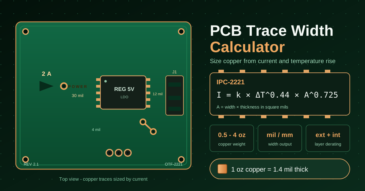
Table of Contents
PCB Trace Width Calculator: Size Copper Traces the IPC-2221 Way
Every copper trace on a printed circuit board is a resistor in disguise. Push enough current through one that is too thin and it warms up, browns the soldermask around it, and in the worst case burns. The cruel part is the timing: a too-thin copper trace is a tiny heater — and the failure shows up months later in the field, long after the board passed its bench test. The PCB Trace Width Calculator catches that mistake at design time, when fixing it costs nothing.
The tool implements the IPC-2221 sizing formulas used across the electronics industry. Enter the current, an allowable temperature rise, the copper weight, and the layer type; it returns the minimum width in mil or mm plus trace resistance, voltage drop, and power dissipation at your trace length. Everything runs 100% client-side, so it works offline and your design never leaves your machine.
This guide walks through the calculator, explains what IPC-2221 assumes, and turns raw numbers into a layout decision you can defend.
Why Use PCB Trace Width Calculator?
- Standards-based math, not folklore. Rules of thumb like "one millimetre per amp" fail on internal layers or in hot enclosures; this applies the IPC-2221 equations reviewers expect.
- External and internal layers handled correctly. A buried trace cannot shed heat like an outer one, and the tool derates it automatically.
- Copper weight from 0.5 to 4 oz. Explore the 1 oz versus 2 oz trade-off instantly instead of guessing.
- Resistance, voltage drop, and power in one place. Long traces still drop voltage and waste power; the outputs quantify both.
- mil and mm output. EDA tools speak mils, fab notes prefer millimetres — you get both.
- Free, offline, and private. No account, no upload; everything computes locally in your browser.
Key Features
| Feature | What It Gives You |
|---|---|
| IPC-2221 formulas | Standard sizing for external and internal layers |
| Current input | Size for worst-case continuous current |
| Temperature rise input | Cap the degrees C the trace may warm |
| Copper weight 0.5-4 oz | The range most fabs quote |
| Width in mil and mm | Straight into your design rules |
| Resistance, voltage drop, power | The electrical cost at any trace length |
| 100% client-side | Instant, offline, nothing sent to a server |
- Temperature rise is a deliberate choice. It forces you to design for the enclosure, airflow, and ambient the board will actually face.
- Electrical outputs update with width. Extra mils of copper visibly buy less wasted energy as you explore.
How to Use
- Enter the design current. Use the worst-case continuous value, including stall or inrush ceilings, not the typical datasheet number.
- Set the allowable temperature rise. 10 °C is conservative; 20-30 °C suits airflow or low duty cycles. The rise adds to ambient, so 10 °C in a 60 °C enclosure means a 70 °C trace.
- Pick the layer. External for outer copper, internal for buried layers; the internal derating is applied for you.
- Select the copper weight. Match what your fab delivers — usually 1 oz, or 2 oz on power boards.
- Read the results. Take the minimum width, then check resistance, voltage drop, and power before rounding up. Rounding 30 mil to 32 mil is cheap insurance; rounding down is not.
Copper, Current, and Heat
The IPC-2221 method rests on one idea: for a given allowed temperature rise, the current a trace can carry depends on its cross-sectional area. The standard writes this as I = k × ΔT^0.44 × A^0.725, where ΔT is the rise in degrees C and A the cross-section in square mils. The constant k — 0.048 external, 0.024 internal — encodes how easily the trace sheds heat; solving for area yields the minimum width the calculator reports.
The layer distinction matters more than newcomers expect. An internal trace sits between glass-epoxy laminates that are good insulators, so its heat escapes by slow conduction instead of convection. The same geometry that carries 2 A on an outer layer is worth roughly half that buried inside — hence the near-doubling of required width when you switch the layer selector.
Copper weight describes foil thickness in ounces per square foot. One ounce plates out to about 1.4 mil, roughly 35 µm; half-ounce is half that, while 2 oz and 4 oz are thicker still. Because cross-section equals width times thickness, heavier copper buys capacity without eating routing channels — a 15 mil trace in 2 oz copper does the work of a 30 mil trace in 1 oz.
Width is only half the electrical story. Copper resistivity gives every trace a resistance proportional to length over cross-section. Run the worked example — 2 A, 10 °C rise, 1 oz external — and the calculator returns about 30 mil, or 0.77 mm. A 100 mm run measures around 63 mΩ: roughly 126 mV dropped and a quarter watt dissipated at 2 A. On a 3.3 V rail that is 4% of the budget gone before the load starts — where the dedicated voltage drop calculator helps audit longer paths.
Two layout details complete the picture. When a power trace changes layers, a single via becomes a bottleneck, so stitch several in parallel rather than let one barrel undo the width you chose. On power pads, thermal reliefs matter too: the spoke pattern saves soldering iron tips, but on very high-current nets solid connections keep the current path cooler.
Practical Use Cases
Power Supply Boards
Regulator outputs, input rails, and star grounds carry the full load continuously. Size them at the regulator's maximum rated output rather than the typical bench load, and the payoff is a board that idles cool instead of browning its soldermask inside a sealed case.
Motor Driver Traces
H-bridge outputs see far more than the nameplate current: stall current can hit two to three times the running figure, plus PWM peaks. Size the phase traces for the stall value, keep them short and symmetric, and let the power dissipation output confirm your heatsinking plan.
LED Strip PCBs
Custom LED boards run one long shared supply trace past every segment, and each centimetre adds resistance that dims the far end. Use the calculator to widen the rail or justify a copper pour, then use the LED resistor calculator to set series resistors once the rail voltage is honest.
Hobby Board Reviews
Before sending an open-source board or a first prototype order to fab, run its power nets through the calculator in two minutes. It is far cheaper than finding the weak trace with a thermal camera after assembly.
Best Practices
- Add margin for manufacturing tolerance. Etching can leave copper 10-20% under nominal, so a paper-exact width is marginal on the panel.
- Keep high-current traces short. Resistance, voltage drop, and heat all scale with length — a shorter route beats a wider one.
- Use copper pours. Flood spare space on power layers and stitch it to the rail for free cross-section and better EMI.
- Check the fab's actual copper spec. "1 oz" often arrives at 1.2-1.3 mil.
- Think in whole-board thermal budgets. A 10 °C rise per trace is fine until five traces share one corner.
- Re-run the numbers each revision. A firmware change that raises current can invalidate a width chosen two spins ago.
Size Your Next Board with Confidence
Some net on your next board will carry more current than you expect. Open the PCB Trace Width Calculator, run every power rail before you route a single trace, and spend ten seconds per net now instead of a re-spin later. It is free, offline, and asks for nothing but your numbers.
Related Tools You Might Like:
- LED Resistor Calculator — size series resistors for LED strings and indicators.
- Ohm's Law Calculator — convert between voltage, current, resistance, and power in seconds.
- Voltage Drop Calculator — audit long cable and trace runs for lost voltage.
Happy routing, and may your traces stay cool!
Frequently Asked Questions
Q: What is IPC-2221 and why does it matter for trace width?
A: It is the generic printed board design standard from IPC. Its current-versus-temperature-rise data and fitted formulas are the de facto baseline reviewers use to judge trace sizing.
Q: What temperature rise should I enter?
A: Base it on environment and criticality: 10 °C is a safe default for sealed products, 20-30 °C for ventilated enclosures or hobby boards. The rise adds to ambient.
Q: Why is the required width larger for internal layers?
A: Internal traces are buried in FR-4, so heat leaves by slow conduction rather than convection. IPC-2221 halves the constant for internal layers, roughly doubling the required width.